Transition Elements as Deep Level Dopant
| ✅ Paper Type: Free Essay | ✅ Subject: Engineering |
| ✅ Wordcount: 3751 words | ✅ Published: 31 Aug 2017 |
HIGH RESISTIVITY SILICON: DEEP-LEVEL DOPING COMPENSATION USING ELEMENTAL GOLD
INTRODUCTION
1.1 Research Background
Monolithic microwave integrated circuit (MMIC) is a microwave circuit in which both active and passive components are fabricated on the same semiconductor substrate [1]. The development of MMICs has been augmented by the high demand for high-speed devices operating at microwave frequency ranging between 300 MHz and 300 GHz. Their advantages of being small, light, and cheap in large quantities have allowed the proliferation of high frequency devices such as cellular phones. However, a problem will arise when standard silicon (Si) substrate is used to operate in super high frequency environment (SHF). The high absorption of microwave power will be caused by the background free carriers present in the substrate [2]. Therefore, low loss and high resistivity substrates are needed to eliminate the problem. It can be achieved by reducing the number of background free carriers in the substrate which result in degradation of circuit performance.
The III-V semiconductor materials such as GaAs, GaN and InP has been widely used in the production of high resistivity substrates due to their wide bandgap nature. However, the wafer diameter produced using III-V materials is typically from 4” to 6” [3]. This increases the cost of production since the standard wafer diameter for modern CMOS technology is 12” [4]. Furthermore, the lattice-mismatch problems will complicate the fabrication process, causing the cost to increase. Therefore, Si has been considered to be an alternative material for the III-V semiconductor compound due to less fabrication complexity and cost. However, the background impurities such as boron will enter the silicon during monocrystalline Si growth causing the increase in substrate losses at microwave range [5].
There have been efforts to use the silicon-on-insulator (SOI) technologies and silicon-on-anything (SOA) to overcome the problem. The SOI wafers can be produced by several methods: silicon-on-sapphire (SOS), separation by implanted oxygen (SIMOX), bond and etch-back SOI (BESOI), Smart Cut™ [6], and epitaxial layer transfer (ELTRAN®) [7]. For SOS approach, a thin film of Si is epitaxially grown on sapphire substrate as shown in figure 1.1. Meanwhile, the other four approaches use a similar cross section of SOI wafer as shown in figure 1.2(b) which consists of three layers: SOI layer (top layer), buried oxide (BOX) layer (middle layer) and silicon substrate (bottom layer). The purpose of the BOX layer is to electrically insulate a fine layer of SOI layer (where the circuits are placed) from the rest of the Si wafer. The SIMOX approach uses implanted silicon dioxide, SiO2 layer as 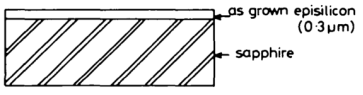
the BOX layer to separate the top thin Si layer from Si substrate.
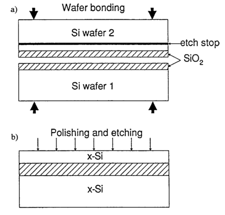
Figure 1.1: Cross-section of silicon-on-sapphire (SOS) wafer [8]
Figure 1.2: A schematic representation of bond and etch-back (BESOI) process [9]
Apart from the mentioned approaches, BESOI, Smart Cut™, and ELTRAN® methods involve the wafer bonding technique. For BESOI method, the thermally oxidised Si wafer (also known as handle wafer) is bonded to another Si wafer which acts as bond wafer as shown in figure 1.2(a). After the wafer bonding process, the top wafer will be etched to obtain the required thickness for SOI layer as shown in figure 1.2(b). On the other hand, implantation of gas ions, most commonly hydrogen is made after the oxidisation process for Smart Cut™ method as shown in figure 1.3. The implantation process is meant for layer splitting process to achieve required thickness of SOI layer after the wafer bonding process. The processes involved in ELTRAN® method is shown in figure 1.4. The ELTRAN® method uses similar procedures in Smart Cut™ with the difference in use of double layer porous Si layer instead of implantation of hydrogen ions. The advantage of using Smart Cut™ and ELTRAN® methods is that the initial wafer or seed wafer can be reused for the same 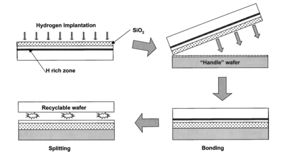
process.
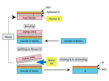
Figure 1.3: Smart Cutâ„¢ process for production of SOI wafers [9]
Figure 1.4: ELTRAN® process flow based on seed wafer reusage [7]
Meanwhile, the SOA technology is achieved by gluing a fully-processed SOI substrate to another substrate such as glass and alumina [10]. However, the on-chip dissipation which could cause thermal breakdown had been proven to be a severe issue [11]. Therefore, there is a need to look for the alternative to SOI and SOA wafers, which is the high resistivity bulk Si substrate. In 2009, International Technology Roadmap for Semiconductors (ITRS) had stressed the importance of high resistivity Si in radio frequency (RF) and analog/mixed signal (AMS) CMOS application [12].
![Figure 1.5: Czochralski crytal puller. CW represent clockwise rotation and CCW represents counter clockwise rotation [13]](https://aaimagestore.s3.amazonaws.com/july2017/0014537.006.png)
There are generally two techniques for Si crystal growth: Czochralski (CZ) technique and float-zone (FZ) technique [13]. A simplified version of CZ puller, which is an apparatus used to produce monocrystalline Si ingots for CZ technique is shown in figure 1.5. The high purity polysilicon, known as electronic grade silicon (EGS) is melted in a rotating silica or quartz crucible. A seed crystal is placed in the melt and then slowly withdrawn from the melt. The molten silicon adhering to the crystal freezes or solidifies into a continuous crystal from the seed. The diameter of the crystal can be maintained by controlling the temperature of the crucible and the rotating speed of the crucible and the rod. However, the CZ process will introduce contamination to the monocrystalline Si due to the presence of oxygen, carbon monoxide and impurities such as boron and phosphorus.
Figure 1.5: Czochralski crytal puller. CW represent clockwise rotation and CCW represents counter clockwise rotation [13]
The FZ process, on the other hand, produces Si crystals with lower contamination as no crucible is used in the process. FZ crystals are mainly used for high power and high voltages devices due to its high resistivity. There is a commercially available high resistivity FZ-Si technology called HiResâ„¢ [14]. The bulk resistivity of Si produced through HiResâ„¢ is up to 70 kΩ-cm, which is suitable for future GHz and THz application. However, it is not suitable for modern CMOS processing since its maximum wafer diameter is limited to 8”, which will increase the cost. Therefore, there is a need to produce high resistivity bulk CZ-Si substrate due to its low fabrication cost. Therefore, CZ process is still the most widely used method in the manufacturing of single crystal silicon.
In 2003, Mallik et al. [2] introduced a new idea in developing a semi-insulating silicon through a method called deep-level doping concentration using 3d transition elements. It showed that there is possibility to produce high resistivity bulk CZ-Si substrate using deep level doping compensation. Following this work, Mallik et al. [5] managed to produce CZ-Si bulk substrate using Mn with resistivity of up to 10 kΩ-cm. Jordan et al. has also used Au to produce CZ-Si wafer with bulk resistivity of up to 180 kΩ-cm [15]. The use of Au-compensated high resistivity bulk Si substrate has been proven by Nur Z. I. Hashim et al. to be able to suppress the parasitic surface conduction (PSC) effect [16].
1.2 Problem Statement
The idea introduced by Mallik et al. [2] on developing high resistivity bulk Si substrate through deep-level doping compensation is solely based on p-type CZ-Si. Even though high resistivity bulk Si substrate has been proven to be achievable using p-type CZ-Si, it has been shown in the work by Jordan et al. [15] that higher magnitude of Au-compensated high resistivity bulk Si substrate can be achieved by using n-type CZ-Si. The potential and problem of using transition elements other than Au as the deep level dopants to produce high resistivity bulk n-type CZ-Si substrate have not been discussed by the work mentioned above.
1.3 Objectives of Research
There are three main objectives that must be met in this research project:
- To investigate the potential of using transition elements as deep level dopant for n-type Si substrate as compared to p-type Si substrate.
- To analyse the result obtained through numerical calculation using MATLAB by comparing it with the experimental data.
- To make a comparative study on the resistivity and effectiveness of the high resistivity bulk substrate produced using n-type CZ-Si with other materials such as III-V semiconductor materials.
1.4 Scope of Research
The scope of this project is to analyse the resistivity plot generated by numerical calculation using MATLAB. The potential and effectiveness of each of the transition elements as deep level dopants for n-type CZ-Si will be discussed in this work. The fabrication and experiment of high resistivity bulk n-type CZ-Si substrate will not be conducted in this work. The experimental data used for comparison with the result of numerical calculation is obtained from Dr. Nur Zatil ‘Ismah Hashim which was done at Southampton Nanofabrication Centre in 2015.

LITERATURE REVIEW
2.1 Introduction
There are several methods to produce high resistivity bulk Si substrate, namely proton implantation method, helium-3 ion irradiation and deep-level doping compensation method. Both proton implantation method and helium-3 ion irradiation use the charge trappings to reduce the current conduction by background free carriers. Meanwhile, the deep-level doping compensation method use the deep dopants to compensate the shallow dopants in the Si substrate.
2.2 Proton Implantation Method
One of the methods to increase the resistivity of CZ-Si substrate is through proton implantation method. The bombardment of protons into Si bulk structure will create defects which can trap mobile carriers. Therefore, the carrier lifetime is low due to the presence of defects, which prevents the mobile carriers from conducting current freely in the substrate. Table 2.1 summarizes the studies conducted to produce high resistivity bulk CZ-Si substrate using proton implantation method.
Table 2.1: Studies on high resistivity bulk CZ-Si substrate using proton implantation method.
|
Contributor |
Year |
Proton Implantation Energy (MeV) |
Resistivity of the Produced Substrate (Ω-cm) |
|
Li |
1989 |
0.18 |
103 |
|
Liao et al. |
1998 |
30 |
106 |
|
Wu et al. |
2000 |
10 |
106 |
|
Rashid et al. |
2002 |
17.4 |
105 |
In 1989, Li [17] managed to produce a high resistivity layer beneath Si surface layer using proton implantation and two-step annealing process. The implantation of proton and annealing process formed the buried defect layer with a resistivity of up to 103 Ω-cm. Meanwhile, Liao et al. created semi-insulating regions within silicon substrate with a resistivity of 1 MΩ-cm [18]. It was achieved by bombarding proton beams at 30 MeV from a compact ion cyclotron to the surface of Si substrate. Following this work, the Si substrate with similar resistivity had been produced by Wu et al. using a lower proton implantation energy, which is 10 MeV [19]. In 2002, Rashid et al. reported a Si substrate with a resistivity of 0.1 MΩ-cm produced through their six-step implantation method using an implantation energy of 17.4 MeV [20].
The high-Q inductors and high transmission gain integrated antenna have been realised on the high resistivity Si substrate by Liao et al. and Rashid et al. respectively [18], [20]. However, the high process cost is needed for proton implantation method as an enormous dose of 1015 cm-2 to maintain the resistivity of the originally 15 Ω-cm Si substrate to be higher than 1014 Ω-cm [21].
2.3 Helium-3 Ion Irradiation Technique
In 1987, helium-3 ion irradiation technique has been used for carrier lifetime control of silicon power devices [22]. The charge trappings created by the helium irradiation and Coulomb scattering of the charged trap will prevent the conduction of current by free mobile carriers in the substrate [23]. Therefore, a high resistivity Si bulk substrate can be realised by the reduction in carrier lifetime.
In 2014, N. Li et al. reported a high resistivity region created within CZ-Si substrate with a resistivity of over 1.5 kΩ-cm using a dose of 1.5×1013 cm-2 of helium-3 ions [24]. The produced high resistivity Si substrate has been used by N. Li et al. in both work for substrate noise isolation improvement in a CMOS process and quality factor improvement in on-chip spiral inductors [24], [25]. R. Wu et al. has also used helium-3 ion irradiation technique in their work on radiation efficiency improvement in 60-GHz on-chip dipole antenna [23].
The helium-3 ion irradiation technique has the advantage of saving the product cost up to 97% as compared to proton implantation method by reducing the dose amount from 1.0×1015 cm-2 to 1.5×1013 cm-2 [24], [25]. However, the helium-3 ion irradiation technique is comparably less studied and the problem associated with this technique has not been discussed in the work mentioned above.
2.4 Deep-Level Doping Compensation Method
![Figure 2.1: Compensation between shallow donors and deep acceptors [26]](https://aaimagestore.s3.amazonaws.com/july2017/0014537.007.png)
The idea of creating high resistivity bulk CZ-Si substrate using deep-level doping compensation has been proposed by Mallik et al. in 2003 [2]. The basic principle of this method is compensating shallow impurities with deep impurities, i.e. shallow donors are being compensated by deep acceptors (as shown in figure 2.1) whereas shallow acceptors are being compensated by deep donors (as shown in figure 2.2).
Figure 2.1: Compensation between shallow donors and deep acceptors [26]
![Figure 2.2: Compensation between shallow acceptors and deep donors [26]](https://aaimagestore.s3.amazonaws.com/july2017/0014537.008.png)
Figure 2.2: Compensation between shallow acceptors and deep donors [26]
As illustrated in figure 2.1, deep acceptors introduced an energy level at EA, which is close to the intrinsic Fermi level. The deep acceptors which are negatively charged attract the minority carrier holes to be trapped at EA level. The electrons from shallow donors are initially excited to the conduction band, then fall to EA level to recombine with the holes. On the other hand, the positively charged deep donors introduced an energy level at ED as shown in figure 2.2. The minority carrier electrons are attracted and trapped at ED level while the holes from shallow acceptors will fall into the valence band. The trapped electrons at ED level then fall into valence band to recombine with the holes. Therefore, there is no generation of free carriers which reduces the resistivity of the substrate in both cases.
Figure 2.3 shows the resistivity of Si at 300K with a background boron concentration of 1014 cm-3, compensated using deep donor impurities with generic energy level positions below conduction band edge, ED. It can be observed that the resistivity of Si increases until a maximum value is reached while the concentration of deep donors, ND increases. The resistivity is low initially due to undercompensation caused by insufficient number of deep donors. The maximum value of the resistivity of Si is reached when deep donors exactly compensate the boron acceptors. Further increase in ND causes overcompensation which results in a fall in the resistivity of Si, making the substrate tends to become n-type.
![Figure 2.3: Calculated resistivity of Si at 300K as a function of generic donor concentration for background boron concentration of 1014 cm-3 [2]](https://aaimagestore.s3.amazonaws.com/july2017/0014537.009.png)
Figure 2.3: Calculated resistivity of Si at 300K as a function of generic donor concentration for background boron concentration of 1014 cm-3 [2]
Table 2.2: Positions of energy levels of transition elements in Si [27]
|
Element |
Donor level below EC (eV) |
Acceptor level above EV (eV) |
|
Co |
0.89 |
0.82 |
|
Pd |
0.84 |
0.9 |
|
Au |
0.78 |
0.56 |
|
Ag |
0.75 |
0.545 |
|
V |
0.45 |
0.92 |
|
Mn |
0.42 |
1.0 |
|
Pt |
0.314 |
0.889 |
It can be noted that the resistivity peaks are sharper for ED which is lower than 0.3 eV while the resistivity remains high over a range of relatively low concentration values for larger values of ED. For small values of ED, almost all donors are ionised and take part in the compensation since the donor energy level is nearer to the conduction band than Fermi level. A slight increase in ND causes the resistivity to decrease sharply, changing the material to n-type. Meanwhile, for large values of ED, the donor level is near intrinsic Fermi level and less fraction of deep donors is ionised. Therefore, the compensation change gradually with the increase in ND and the resistivity remain high over a wide range of ND.
The transition elements are used as deep level dopants as they introduce a pair of deep donor and deep acceptor levels into the Si band gap as shown in table 2.2. The deep dopant energy levels introduced by the transition elements pin the Fermi level near the middle of the Si band gap as shown in figure 2.4 [15]. Thus, high resistivity CZ-Si substrate can be achieved by capturing the free carriers by deep impurities, which reduces the concentration of background free carrier.
![Figure 2.4: Fermi level pin by deep levels introduced by transition elements [15]](https://aaimagestore.s3.amazonaws.com/july2017/0014537.010.png)
Figure 2.4: Fermi level pin by deep levels introduced by transition elements [15]
![Figure 2.5: Calculated resistivity of Si at 300K as a function of Au, Ag, Co and Pd for three different background boron concentration in cm-3 [2]](https://aaimagestore.s3.amazonaws.com/july2017/0014537.011.png)
Figure 2.5: Calculated resistivity of Si at 300K as a function of Au, Ag, Co and Pd for three different background boron concentration in cm-3 [2]
![Figure 2.6: Calculated resistivity of Si at 300K as a function of (a) Pt (b) V and (c) Mn concentrations for three different background boron concentrations in cm-3 [2]](https://aaimagestore.s3.amazonaws.com/july2017/0014537.012.png)
Figure 2.6: Calculated resistivity of Si at 300K as a function of (a) Pt (b) V and (c) Mn concentrations for three different background boron concentrations in cm-3 [2]
![Figure 2.7: Calculated resistivity of Si as a function of Au concentration for n-type and p-type Si with a shallow doping concentration of 1014 cm-3 [28]](https://aaimagestore.s3.amazonaws.com/july2017/0014537.013.png)
Figure 2.7: Calculated resistivity of Si as a function of Au concentration for n-type and p-type Si with a shallow doping concentration of 1014 cm-3 [28]
The transition element dopants are generally grouped into two categories: Au, Ag, Co and Pd are in first category whereas Pt, V and Mn are in second category. As illustrated in figure 2.5, the resistivity of p-type CZ-Si substrate increases with increasing concentration of the deep dopants in first category. The behaviour of impurities in first category is due to presence of both deep donor and acceptor levels very near intrinsic Fermi level of Si bandgap. For Au and Ag, the resistivity of Si reaches a plateau at the concentration of deep dopants over 1016 cm-3 for three different background boron concentration. The reason for the slight difference in the behaviour of Au and Ag is that the both donor and acceptor level is nearer to the middle in the Si bandgap as compared to Co and Pd.
For the second category of deep dopants, the resistivity of p-type CZ-Si reaches a peak and then reduce sharply with the increase in the concentration of the deep dopants as shown in figure 2.6. The reason of the difference in the behaviour is that the impurities in second category have either donor or acceptor level near the intrinsic Fermi level. Therefore, the dopants in second category can only compensate for a single type of doped silicon substrate.
The effect of using 3d transition elements as deep level dopants in n-type CZ-Si substrate has not been shown in the work by Mallik et al. Meanwhile, it is shown in the work by Jordan et al. that higher bulk resistivity of Au-compensated Si substrate can be achieved by using n-type CZ-Si as shown in figure 2.7 [28]. The n-type Au-compensated Si substrate with resistivity up to 70 kΩ-cm has been used by Nur Z. I. Hashim et al. for realisation of coplanar waveguides (CPW) on the substrate [29]. Therefore, the potential and problem of using 3d transition elements for deep-level compensation in n-type CZ-Si substrate will be discussed in this work.
2.5 Summary
The realisation of high resistivity bulk Si substrate using proton implantation method and helium-3 ion irradiation technique was studied. The fabrication of high-Q inductors and antenna has been done on the Si substrate produced using both methods. However, there are problems associated with both methods such as high product cost for proton implantation method and being comparably less studied for helium-3 ion irradiation. Therefore, the idea of creating a semi-insulating silicon substrate using deep-level doping compensation with 3d transition elements was proposed by Mallik et al. in 2003. The deep-level doping compensation method has since been well studied and used for the fabrication of coplanar waveguides and inductors by Nur Z. I. Hashim et al.
References
- [1]I. D. Robertson and S. Lucyszyn, RFIC and MMIC Design and Technology. IET, 2001.
- [2]K. Mallik, R. J. Falster, and P. R. Wilshaw, “‘ Semi-insulating ‘ silicon using deep level impurity doping: problems and potential,” Semicond. Sci. Technol., vol. 18, no. 6, p. 517, 2003.
- [3]”Products & Capabilities | EpiWorks,” EpiWorks. [Online]. Available: http://www.epiworks.com/products-capabilities/. [Accessed: 28-Feb-2017].
- [4]”Global Manufacturing at Intel,” Intel. [Online]. Available: http://www.intel.co.uk/content/www/uk/en/architecture-and-technology/global-manufacturing.html?wapkw=wafer+size&_ga=1.16867193.1775779534.1436014173. [Accessed: 28-Feb-2017].
- [5]K. Mallik, C. H. De Groot, P. Ashburn, and P. R. Wilshaw, “Enhancement of resistivity of Czochralski silicon by deep level manganese doping,” Appl. Phys. Lett., vol. 89, no. 11, p. 3, 2006.
- [6]”Smart Cut technology, Smart Choice – Soitec,” Soitec. [Online]. Available: https://www.soitec.com/en/products/smart-cut. [Accessed: 28-Feb-2017].
- [7]T. Yonehara and K. Sakaguchi, “ELTRAN ® ; Novel SOI Wafer Technology,” vol. 4, no. 4, pp. 10-16, 2001.
- [8]S. Iwamatsu and M. Ogawa, “Silicon-on-sapphire m.o.s.f.e.t.s fabricated by back-surface laser-anneal technology,” Electron. Lett., vol. 15, no. 25, pp. 827-828, 1979.
- [9]G. K. Celler and S. Cristoloveanu, “Frontiers of silicon-on-insulator,” J. Appl. Phys., vol. 93, no. 9, pp. 4955-4978, 2003.
- [10]R. Dekker, P. G. M. Baltus, and H. G. R. Maas, “Substrate transfer for RF technologies,” IEEE Trans. Electron Devices, vol. 50, no. 3, pp. 747-757, 2003.
- [11]N. Nenadovic, V. D’Alessandro, L. K. Nanver, F. Tamigi, N. Rinaldi, and J. W. Slotboom, “A back-wafer contacted silicon-on-glass integrated bipolar process. Part II. A novel analysis of thermal breakdown,” IEEE Trans. Electron Devices, vol. 51, no. 1, pp. 51-62, 2004.
- [12]”RF and AMS tech for wireless communications,” International Technology Roadmap for Semiconductors, 2009. [Online]. Available: http://www.itrs2.net/itrs-reports.html. [Accessed: 28-Feb-2017].
- [13]S. M. Sze, Semiconductor Devices: Physics and Technology, 2nd ed. New York: John Wiley and Sons, 2002.
- [14]”High resistivity silicon for GHz and THz technology,” Topsil. [Online]. Available: http://www.topsil.com/en/silicon-products/silicon-wafer-products/hiresTM.aspx. [Accessed: 28-Feb-2017].
- [15]D. M. Jordan, R. H. Haslam, K. Mallik, and P. R. Wilshaw, “The Development of Semi-Insulating Silicon Substrates for Microwave Devices,” Electrochem. Soc., vol. 16, no. 6, pp. 41-56, 2008.
- [16]N. Z. I. Hashim, A. Abuelgasim, and C. H. De Groot, “Suppression of parasitic surface conduction in Au-compensated high resistivity silicon for 40-GHz RF-MMIC application,” 2014 Asia-Pacific Microw. Conf., pp. 55-57, 2014.
- [17]J. Li, “Novel semiconductor substrate formed by hydrogen ion implantation into silicon,” Appl. Phys. Lett., vol. 55, no. 21, pp. 2223-2224, 1989.
- [18]C. Liao et al., “Method of creating local semi-insulating regions on silicon wafers for device isolation and realization of high-Q inductors,” IEEE Electron Device Lett., vol. 19, no. 12, pp. 461-462, 1998.
- [19]Y. H. Wu et al., “Fabrication of very high resistivity Si with low loss and cross talk,” IEEE Electron Device Lett., vol. 21, no. 9, pp. 442-444, 2000.
- [20]A. B. M. H. Rashid, S. Watanabe, and T. Kikkawa, “High transmission gain integrated antenna on extremely high resistivity Si for ULSI wireless interconnect,” IEEE Electron Device Lett., vol. 23, no. 12, pp. 731-733, 2002.
- [21]L. S. Lee et al., “Isolation on Si wafers by MeV proton bombardment for RF integrated circuits,” IEEE Trans. Electron Devices, vol. 48, no. 5, pp. 928-935, 2001.
- [22]W. Wondrak and A. Boos, “Helium Implantation for Lifetime Control in Silicon Power Devices,” ESSDERC ’87 17th Eur. Solid State Device Res. Conf., pp. 649-652, 1987.
- [23]R. Wu et al., “A 60-GHz efficiency-enhanced on-chip dipole antenna using helium-3 ion implantation process,” 2014 44th Eur. Microw. Conf., pp. 108-111, 2014.
- [24]N. Li et al., “High-Q inductors on locally semi-insulated Si substrate by helium-3 bombardment for RF CMOS integrated circuits,” 2014 Symp. VLSI Technol. Dig. Tech. Pap., pp. 1-2, 2014.
- [25]N. Li et al., “Substrate noise isolation improvement by helium-3 ion irradiation technique in a triple-well CMOS process,” 2015 45th Eur. Solid State Device Res. Conf., pp. 254-257, 2015.
- [26]J. D. Puksec and V. Gradisnik, “Influence of shallow impurity on steady-state probability function of multilevel deep impurity,” 2000 10th Mediterr. Electrotech. Conf. Inf. Technol. Electrotechnol. Mediterr. Countries. Proc., vol. I, pp. 185-188, 2000.
- [27]W. Schroeter and M. Seibt, “Deep Levels of Transition Metal Impurities in c-Si,” in Properties of Crystalline Silicon, R. Hull, Ed. London: INSPEC IEE, 1999, p. 561.
- [28]D. M. Jordan, K. Mallik, R. J. Falster, and P. R. Wilshaw, “Semi-Insulating Silicon for Microwave Devices,” Solid State Phenom., vol. 156-158, pp. 101-106, 2009.
- [29]N. Z. I. Hashim, A. Abuelgasim, and C. H. De Groot, “Coplanar waveguides on gold-doped high resistivity silicon for 67-GHz microwave application,” RFM 2013 – 2013 IEEE Int. RF Microw. Conf. Proc., pp. 274-277, 2013.
Cite This Work
To export a reference to this article please select a referencing stye below:
Related Services
View all


DMCA / Removal Request
If you are the original writer of this essay and no longer wish to have your work published on UKEssays.com then please click the following link to email our support team:
Request essay removal