Room Temperature Synthesis and Optical Properties of Nanostructured Ba-Doped ZnO Thin Films
| ✅ Paper Type: Free Essay | ✅ Subject: Sciences |
| ✅ Wordcount: 4622 words | ✅ Published: 23 Sep 2019 |
Room Temperature Synthesis and Optical Properties of Nanostructured Ba-Doped ZnO Thin Films
Abstract
Zinc oxide films with and without barium-doping have been prepared by the SILAR technique with different percentages (1 M%, 3 M%, 5 M% and 7 M%) of Ba content on microscopic glass slides. The effects of the concentration of barium doped on zinc oxide (BaZO) were characterized by X-ray diffraction (XRD), UV-Vis Spectroscopy, Scanning Electron Microscopy (SEM) and Energy Dispersive X ray (EDX).The XRD studies confirmed that the structural growth of ZnO films were polycrystalline in nature. The Ba doped ZnO films deposited were found to have strong orientation at (002) lattice plane which exhibited polycrystalline hexagonal wurtzite structure. The SEM showed that the grain size, thus the roughness, increased as a result of increase in the level of barium doping. Optical bandgaps obtained decreased from 3.41 eV to 3.19 eV with an increase in Ba concentration.
Keywords: Ba-Zinc Oxide; SILAR Technique; Thin films; optical properties; SEM; XRD.
- Introduction
For many years, the synthesis and characterization of ZnO thin films have been an interesting area of research. The wurtzite structure of ZnO forms an n-type semiconductor with direct band gap
of about 3.37eV at a temperature of 300K [1], and high electronic mobility. As a wide and direct band gap semiconductor, ZnO thin films have attracted more and more attention in optoelectronic devices [2–5], photo-thermal conversion systems, heat mirrors, blue/UV light electrode devices, solid state detectors, crystal clear electrodes, heterojunction solar cells etc [6–10]. Undoped ZnO thin films have definite restrictions in their usage. In order to broaden the potential areas where ZnO thin films can be used, dopant ions have to be integrated into them to obtain definite desired properties like lower or higher melting point, broader or narrower band gap, higher optical absorbance, etc. by applying different techniques.
Different techniques have been applied to obtain ZnO nanostructured thin films such as RF magnetron sputtering [11], chemical vapour deposition [12], chemical bath deposition [13], pulse laser deposition [14]. Others include spray pyrolysis [15], sol-gel process [16], chemical co-precipitation [17], hydrothermal [18], ultrasonic irradiation assisted solution route [19], solid-state reaction [20], successive ionic layer adsorption and reaction (SILAR) [21,22],etc. Among these techniques, SILAR technique has lately attracted appreciable attention because of its low cost and simplicity. Furthermore, this technique requires low temperatures and facilitates large-area deposition.
In recent work, an attempt has been made to synthesize Ba doped ZnO thin films by SILAR technique, since it involves adsorption of a layer of complex ion on the substrate after that reaction of the adsorbed ion layer [23]. Ba doped ZnO is an important technological material used for example in varistors and liquid sensors’ guiding layers[24]. Precisely, doping ZnO with Ba procures to ZnO films a rougher surface, a stronger internal stress, and a low density crystalline structure [25].This paper investigates the effect of varying percentage of barium (Ba) as a dopant on zinc oxide (ZnO) thin films synthesized by SILAR method with ZnSO4.2H2O and BaCl2 as precursor and dopant materials respectively.
-
Experimental Details
- Substrate cleaning
For deposition of ZnO films on glass slides, SILAR technique was used. The clean glass slides (micro slide-25.4 mm wide × 76.2 mm lengths and thickness 1mm-1.2mm) were soaked in acetone (to degrease the substrates from any possible stains) for 30 minutes. They were rinsed again with distilled water and ultrasonicated for 20 minutes. Finally, they were dried in a thermo-blast furnace for 20 minutes at 60oC. The cleaned glass slides were gently safe guarded in a clean glass slides pack.
2.2 Synthesis procedure
The un-doped ZnO film was deposited as stated below: Firstly, 0.8M concentration of hydrated zinc sulphate (ZnSO4.2H2O) was prepared with aqueous ammonia (NH4OH, 29%) and 50ml distilled water. The aqueous solution was then stirred thoroughly by mixing it with a magnetic stirrer for about 20 minutes for it to dissolve completely to produce a colourless aqueous solution of [Zn(NH3)4]2+ (Zinc(II) tetra-amine ion) cationic precursor. The aqueous ammonia added to the resultant mixture helps to modify the pH solution to 8.1. For the growth of ZnO (intrinsic semiconductor) films, 40 cycles were carried out in each case.
Secondly, in case of Ba doped ZnO (BaZO) (extrinsic semiconductor) thin films, a measured amount of barium chloride (Bacl2) were added to the initial solution in separate beakers. In order to determine the effect of varying percentages of barium (Ba) as a dopant on ZnO thin films, we conducted the experiments at five different concentrations. Ba2+ ions were added to the deposition beakers at1 M%, 3 M%, 5 M% and 7 M%. Water bath was used as an anionic precursor in order to reduce temperature fluctuation.

The summary of the procedure for depositing ZnO films at 40 cycles are shown below:
- The clean glass slides were dipped in the complex aqueous of zinc (II) tetra-amine ion [Zn(NH3)4]2+(cationic precursor) kept at room temperature for 30s;
- Immediately the precipitates of Zn(OH)2 were found on the glass slides, the glass slides were dipped in distilled water at room temperature for 30s;
- The glass slides were immersed dipped in hot distilled water bath maintained at 70oC to 80oC for 30s to adsorb oxygen and generate ZnO;
- The glass slides were sonicated for 30s in distilled water at room temperature in order to separate the counter ions S042- from loosely precipitated Zn(OH)2 grains.
Figure 1: Experimental set up for SILAR technique.
2.3 Reactions equations
From equations (1) – (5), it exemplifies a chemical reaction connected with both un-doped and doped process:
Un-doped process:
ZnSO4.2H2O + 2NH4OH = Zn(OH)2 + (NH4)2SO4 + 2H2O (1)
Zn(OH)2 + 4NH3.H2O = [Zn(NH3)4]2+ + 2OH– + 4H2O (2)
It was deduced from the process of the anionic reaction, complex aqueous solution of zinc (II) tetra-amine ions, broke up with Zn(OH)2 precipitation:
[Zn(NH3)4]2+ + 4H2O = Zn(OH)2 ↓ + 4NH4 + 2OH– (3)
Therefore Zn(OH)2 = ZnO + H2O (4)
Doped process:
[Zn(NH3)4]2+ + BaCl2.2H2O = [ZnBa(NH3)4]2+ + Cl2 (5)
2.4 Characterisation
SEM, XRD, UV-Vis and EDX analysis were performed in order to figure out the morphological, structural, optical analysis and elemental compositions of ZnO films. Crystal structures of the films were ascertained by an XRD over the range of 2
o. The optical analysis of the films was determined by UV-Vis spectrophotometer at room temperature over the range of 200 – 1000nm.
3. Results of the experiment and discussion
3.1 Structural characterisation
Crystallographic analysis of ZnO films was determined using XRD technique. Figure 2 shows the x-ray diffraction plots of un-doped ZnO (intrinsic semiconductor) and barium doped ZnO (extrinsic semiconductor) films deposited on glass substrates at various concentrations of doping (1 M%, 3 M%, 5 M% and 7 M%). Several diffraction peaks were noticed. These diffraction peaks show the polycrystalline nature of the films[26].
Diffractograms indicated that barium doped ZnO (BaZO) films were only incorporated in the lattice plane of ZnO. For Ba-doped ZnO (BaZO) (extrinsic semiconductor) films, prominent peaks were showed at 2
= 31.7o, 34.5o, 36.3o, 47.6o, 56.7o,62.8o and 67.8o which corresponds to (100), (002), (101), (102), (110), (103) and (112) lattice planes respectively except un-doped ZnO films which showed a peak only at the (100) lattice plane. An increase in Ba concentration showed an increase in the intensity at the (002) plane.This result shows that Ba atoms act as donors in ZnO films thereby donating extra valence electrons to the conduction band of semiconductor, which provided excess electrons to un-doped ZnO which makes it to be an n-type semiconductor.
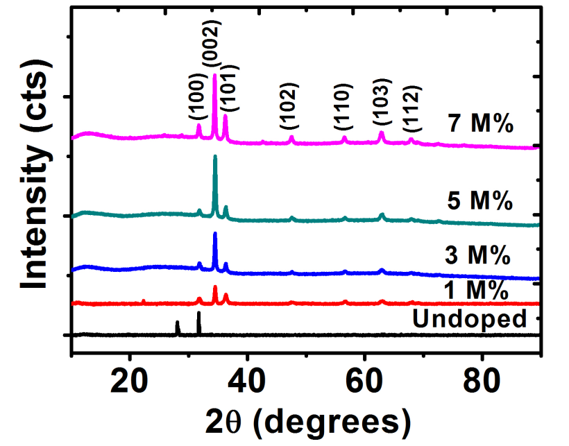
Figure 2: The XRD pattern for undopedZnO and Ba doped ZnO .
Table 1 shows the different parameters calculated from the XRD diffraction plots. Theaverage crystallite size was calculated from the XRD using Scherrer’s formula [27,28]:
(6)
Where λ, θ andβ are the wavelength, Bragg’s diffraction angle andfull width at half maximum,respectively.The un-doped crystallites presented a much higher size than those of the Ba-doped samples. The crystallite sizes of the ZnO at different dopant concentration ranged from 30.4 to 33.6 nm. However, there is no clear trend observed as the concentration increases.
The inter-planar distance, d, which is the vertical spacing between parallel atomic planes in a crystal was calculated using equation (7)[29].
 (7)
(7)
The lattice strain, ε, which is as a result of distortion and inhomogeneity was calculated using the equation (8)[30].
 (8)
(8)
The dislocation density was obtained using equation (9)[31]
 (9)
(9)
There was a sharp decrease in crystallite sizes from 82.22 nm for undopedZnO to 30.43 nm for Ba doped ZnO at 1 M%. However, there is no evidence that an increase in the dopant concentration increased or decreased the crystallite sizes as no such trend is observed.
Table 1: Crystallographic parameters of undopedZnO and Ba doped ZnO .
|
Ba Concentration |
FWHM (0) |
D (nm) |
d (nm) |
ε (x10-3) |
δ (x10-4 nm-2) |
|
Undoped |
0.1004 |
82.2167 |
0.281 |
1.539 |
1.48 |
|
1 M% |
0.2733 |
30.4258 |
0.260 |
3.841 |
10.80 |
|
3 M% |
0.2510 |
33.1290 |
0.260 |
3.528 |
9.11 |
|
5 M% |
0.2727 |
30.4955 |
0.259 |
3.529 |
10.75 |
|
7 M% |
0.2616 |
31.7807 |
0.260 |
3.685 |
9.90 |
3.3 Surface morphology and chemical compositions
These micrographs showed that the surfaces of BaZO films improved by doping process. A change in the grain size due to varying percentages of dopant was noticed. Fig 3(a) shows an arrangement of highly dense and agglomerated undoped ZnO in budlike form. Introduction of Ba dopant in smaller concentrations (1-3 M%) produced more evenly dispersed nanostructures with no change in the budlike shape. Further increase in the concentration (5-7 M%) revealed the formation of nanorods.
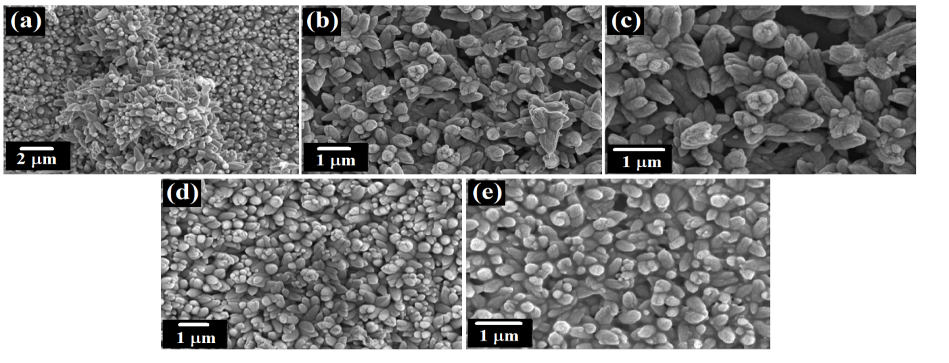
Fig. 3: SEM images of (a) undopedZnO; Ba doped ZnO at (b) 1 M%; (c) 3 M%; (d) 5 M% and (e) 7 M%.
The number of cycles play a huge role in the agglomeration of the nanoparticles. As illustrated in figure 4 at lower deposition cycles, the sparsely distributed nanostructures will be formed. Increasing the number of cycles results in more densely packed nanostructure while increasing the film thickness. In our case, 40 cycles produce highly agglomerated nanoparticles irrespective if the dopant concentration.
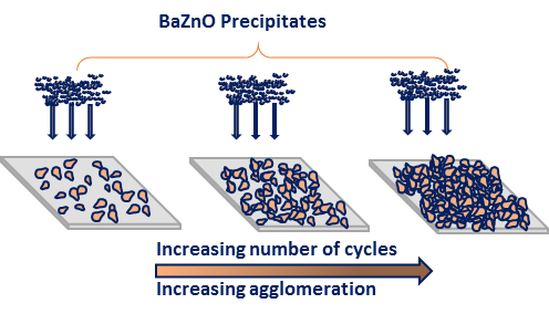
Figure 4: Growth formation of Ba doped ZnO nanoparticles using SILAR method.
The compositions of the elements of ZnO films were studied using EDX as shown in figure5. For all doped samples, peaks of oxygen (O), calcium (Ca), barium (Ba) and silicon (Si) exhibit the presence of these elements in the deposited thin films. Also for all samples, zinc element has a higher ratio when compared to oxygen (O) element. The peaks of silicon originated from the glass substrate. The EDX pattern confirmed Zn and O and hence ZnO deposited. Apart from the key elemental composition, the appearance of other elements such as silicon Si, C, and Ca, on the EDX pattern is as a result of glass substrates used during deposition period contained silicon (Si) which belongs in the same group with carbon (C) in the periodic table and barium (Ba) used as a dopant and it belongs to the same group with calcium (Ca) in the periodic table.
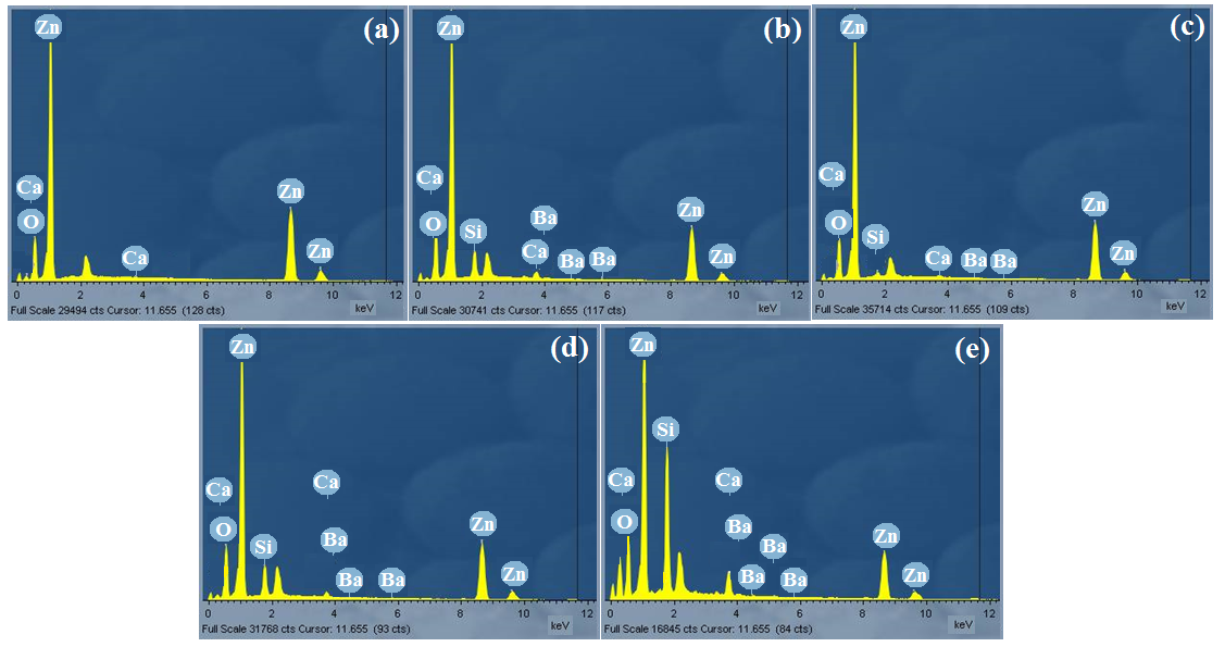
Fig. 5: EDX graphs of (a) undopedZnO; Ba doped ZnO at (b) 1 M%; (c) 3 M%; (d) 5 M% and (e) 7 M%.
3.2 Optical properties
The undopedZnO thin film has the highest band gap when compared with those of 1 M%, 3 M%, 5 M% and 7 M% doped as shown in fig. 6 (a-e). As represented in fig. 6(f), the values of band gaps of ZnO film decreased with increase in percentages of doping. This decrease in band gap can be used to improve the visible light capturing in solar cell applications[32].
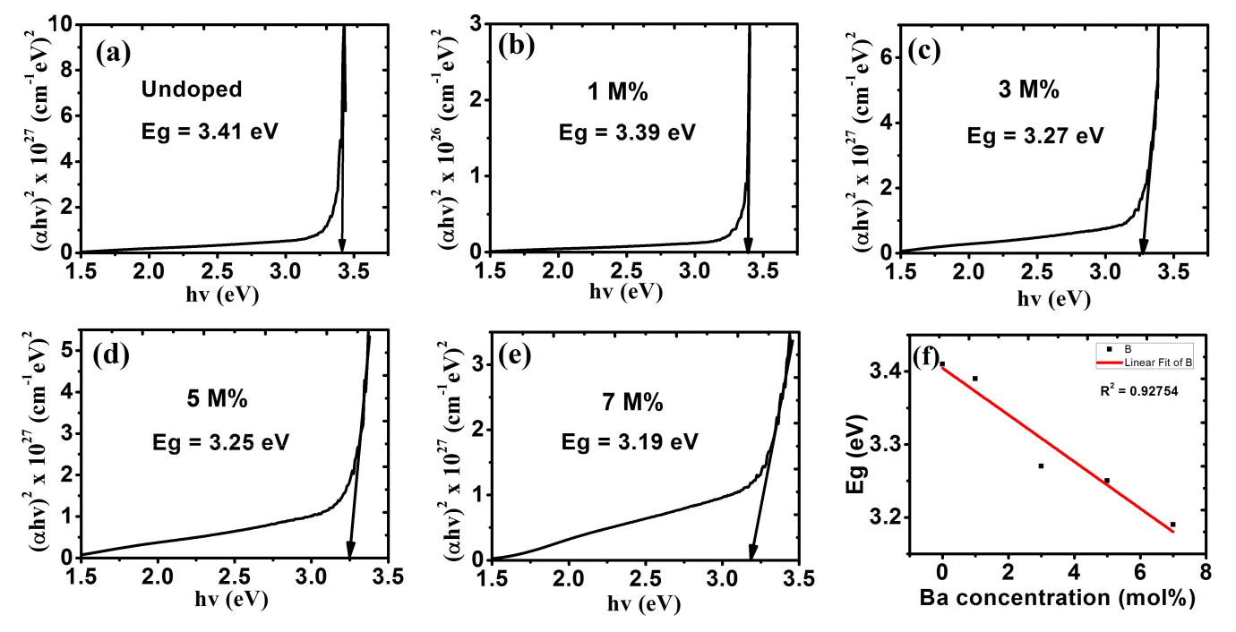
Figure 6: Energy band gap for (a) undoped ZnO; Ba doped ZnO at (b) 1 M%; (c) 3 M%; (d) 5 M% and (e) 7 M%.
(f) Shows a plot of the decreasing bandgap with increased Ba concentration.
The transmittance of the films is shown in figure 7.The films presented a relatively low transmittance in the visible light region with the highest transmittance being the Ba-doped ZnO at 1 M%. Further increase in the dopant concentration showed a decline in the transmittance. The transmittance for all the films proportionally increased at the NIR region and could possibly be used as material for poultry roofs and walls [33].
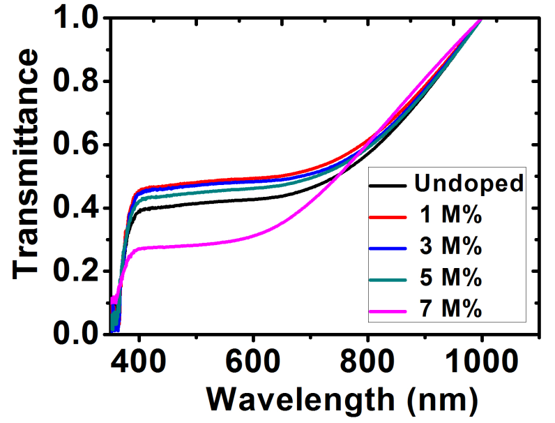
Figure 7: Transmittance spectra for ZnO and Ba doped- ZnO films.
The average refractive indices of 2.64, 2.62, 2.63, 2.64 and 2.45 in the visible light region (400 nm – 700 nm) were obtained for the undoped ZnO, Ba doped ZnO at 1 M%, 3 M%, 5 M% and 7 M% respectively (figure 8(a)). According to Pushparajah et al (1994), the refractive index of ZnO films doped with Li deposited by spray pyrolysis lie between 1.60 and 2.20 at a wavelength of 500 nm [34] while according to the report made by Ezema (2004) gave the average refractive index of the ZnO films deposited by chemical bath method as being between 1.64 and 1.98 and also reported observed peak values of 2.28 at 368 nm and 1.72 at 569 nm [35]. Figure 8(b) shows an increase in extinction coefficient with an increase in dopant concentration.
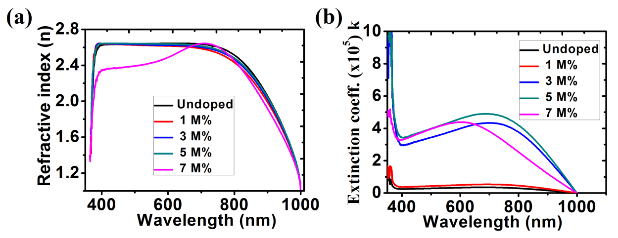
Fig. 8: (a) Refractive index; (b) Extinction Coefficient for ZnO and Ba doped ZnO films.
The optical absorbance was recorded by using a single beam spectrophotometer from the wavelength range 350 nm to1000 nm shown in fig. 9(a). From the graph, it is observed that absorption spectrum of ZnO thin films decreases as wavelength increased. The absorbance values were calculated with wavelengths in the range of 390 nm to1000nm in the visible region. The results show that 7 M% Ba doped ZnO has the highest absorbance in the visible light region. Figure 9(b) shows a plot of absorption coefficient (α) versus wavelength. It can be calculated from expression [36]:
α =
(10)
A represent the absorbance and t represent the thickness. From the graph, it is observed that the absorption coefficient decreased with increase in wavelength (380 nm to 1000 nm) in the visible region.
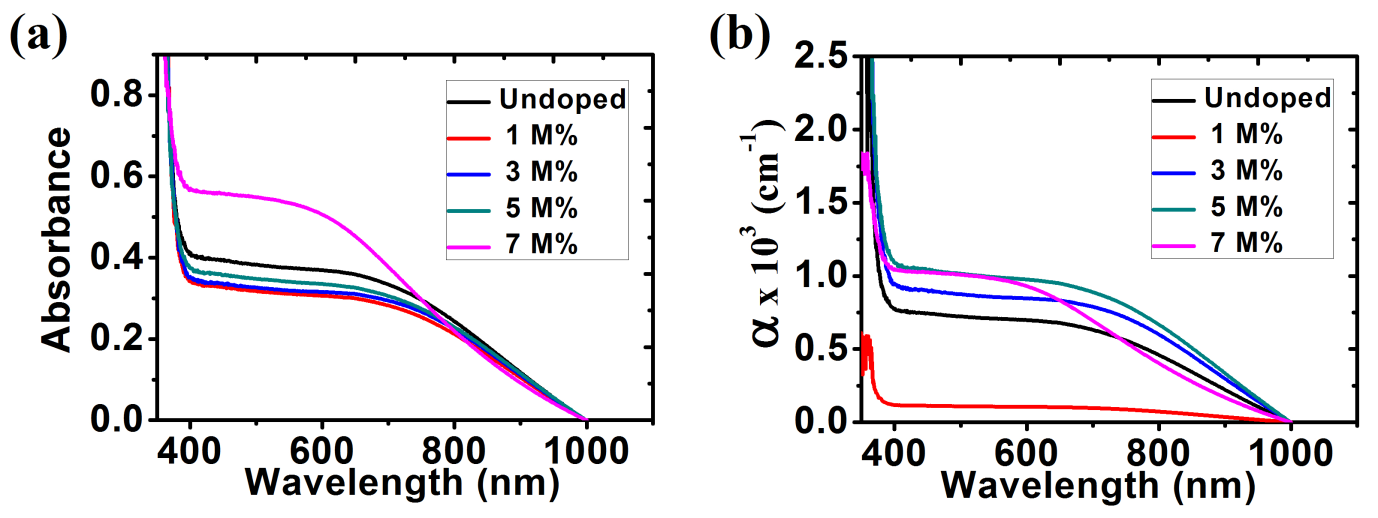
Fig. 9: (a) Absorbance; (b) Absorption coefficient for ZnO and Ba doped ZnO films.
Fig. 10 (a) shows optical reflectance spectra of different samples of ZnO thin films. It is observed that the reflectance of all the deposited thin films is low. The lowest reflectance in the visible light region was observed at the highest Ba concentration (7 M%). This low reflectance value makes ZnO thin film is an important material for anti-reflection coating.
The change in optical conductivity with photon wavelength showed that the optical conductivity decreased with increase in the photon wavelength in the visible region as seen in fig. 10 (b).
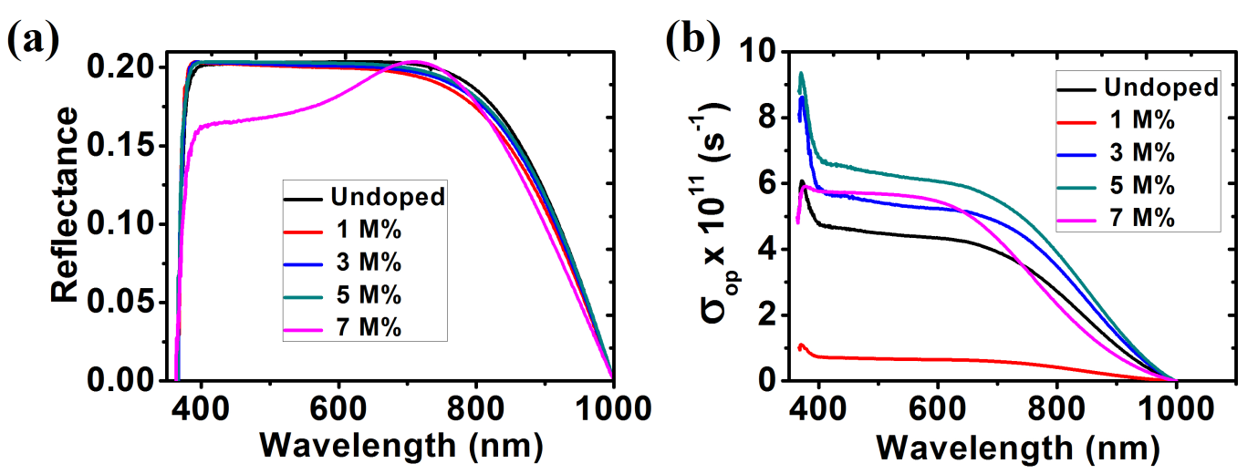
Fig. 10: (a) Reflectance; (b) Optical Conductivity for ZnO and Ba doped ZnO films.
The refractive index values were used to obtain some dielectric properties such as the lattice dielectric constant εL and plasma frequency ωp using the relation in equation (11) [37]
 (11)
(11)
Where, n is the refractive index, εL is the lattice dielectric constant, ωp is the plasma frequency and c is the speed of light. A plot of n2 against λ2 as shown in figure 11(a) yields εL as the intercept while ωp is calculated from the slope. Table 2 shows the calculated values of these parameters at different dopant concentrations. An increase in Ba concentration led to a near constant lattice dielectric constant while there was a decrease in the plasma frequency. This decrease in plasma frequency implies that there could be a decrease in the charge carrier density as the dopant concentration increases. The plasma frequency indicates the shift from a dielectric to a metallic property in materials. If the frequency of light incident on the material is greater than the plasma frequency, the light is easily transmitted through the material. Consequently, at lower incident light frequencies, the light will be reflected[38].
The oscillation energy Eo and dispersion energy Ed were obtained using the Wemple and Di Domenico model [39] in equation (12).
 (12)
(12)
A plot of  against
  in figure 11(b) produces a slope and intercept of
  and
and , respectively, from which Ed and Eo were easily calculated and values represented in Table 2. Both the oscillation energy and the dispersion energy decreased with increased concentration. This is in contradiction with [38] which attributes the decrease in Eo to a decrease in energy band gap Eg.
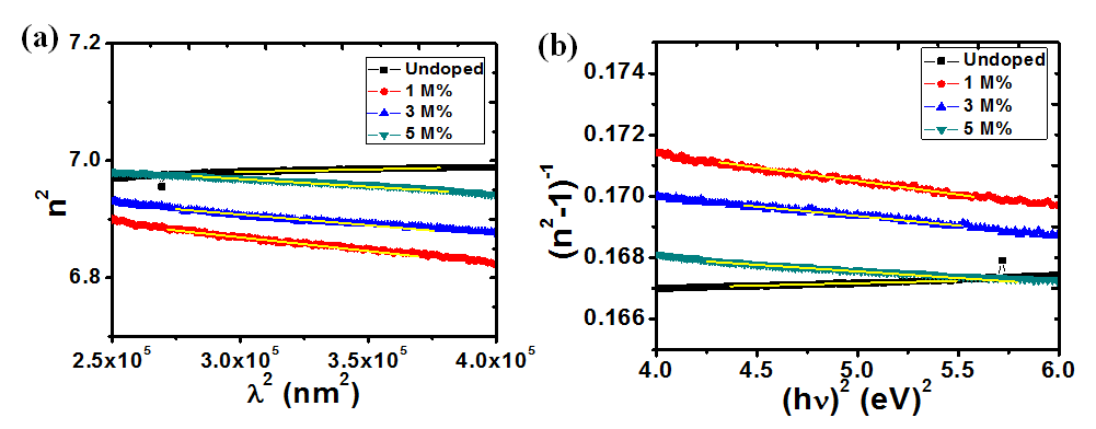
Figure 11: Plots (a) n2 vs λ2and (b) (n2-1)-1 vs (hv)2 for calculating the dielectric and optical dispersion parameters, respectively.
Table 2: Summary of the optical constants and dispersion parameters of ZnO and Ba doped ZnO at different molar concentrations.
|
Dopant concentration (M%) |
n |
Eg (eV) |
ωp(105 s-1) |
εL |
Ed (eV) |
Eo (eV) |
|
Undoped |
2.64 |
3.41 |
3.47 |
6.955 |
221.04 |
36.78 |
|
1 |
2.62 |
3.39 |
7.40 |
7.006 |
78.04 |
13.63 |
|
3 |
2.63 |
3.27 |
6.27 |
7.012 |
98.85 |
17.05 |
|
5 |
2.64 |
3.25 |
5.27 |
7.046 |
124.67 |
20.92 |
4. Conclusion
Undoped and Ba doped ZnO thin films with different percentages (1 M%, 3 M%, 5 M% and 7 M%) of Ba content have been successfully synthesized by SILAR technique on glass substrates. The XRD studies confirmed the growth of ZnO thin films with polycrystalline hexagonal wurtzite structure with a preferential orientation of (002) plane for all samples.
The SEM imagesindicated that the grain size, thus the roughness, increasedin proportion with Ba doping level. Optical analysis showed that an optical band gap of ZnO films (undoped and doped) reduced from 3.41eV to 3.19 eV with increased Ba dopant concentration. An increase in Ba concentration led to a decrease in the plasma frequency while there was a decrease in both the oscillator energy and the dispersive energy. In summary, this study reveals the tunability of the optical parameters on ZnO by varying the barium dopant concentration.
REFERENCES
- [1] M. Nirmala, A. Anukaliani, Structural and optical properties of an undoped and Mn doped ZnO nanocrysatlline thin film, Photonics Lett. Pol. 2 (2010) 189–191.
- [2] G. Xiangdong, L. Xiaomin, Y. Weidong, Preparation and characterization of highly oriented ZnO film by ultrasonic assisted SILAR method, J. Wuhan Univ. Technol.-Mater Sci Ed. 20 (2005) 23–26.
- [3] T. Yen, D. Strome, S.J. Kim, A.N. Cartwright, W.A. Anderson, Annealing studies on zinc oxide thin films deposited by magnetron sputtering, J. Electron. Mater. 37 (2008) 764–769.
- [4] V. Shelke, B.K. Sonawane, M.P. Bhole, D.S. Patil, Electrical and optical properties of transparent conducting tin doped ZnO thin films, J. Mater. Sci. Mater. Electron. 23 (2012) 451–456.
- [5] B. Zhou, A.V. Rogachev, Z. Liu, D.G. Piliptsou, H. Ji, X. Jiang, Effects of oxygen/argon ratio and annealing on structural and optical properties of ZnO thin films, Appl. Surf. Sci. 258 (2012) 5759–5764.
- [6] T. Negami, Y. Hashimoto, S. Nishiwaki, Cu (In, Ga) Se2 thin-film solar cells with an efficiency of 18%, Sol. Energy Mater. Sol. Cells. 67 (2001) 331–335.
- [7] Y. Natsume, H. Sakata, Zinc oxide films prepared by sol-gel spin-coating, Thin Solid Films. 372 (2000) 30–36.
- [8] X. Wang, W.P. Carey, S.S. Yee, Monolithic thin-film metal-oxide gas-sensor arrays with application to monitoring of organic vapors, Sens. Actuators B Chem. 28 (1995) 63–70.
- [9] S. Roy, M. Boro, D. Mohanta, A. Choudhury, G.A. Ahmed, Size quantification of sub-micron ZnSe semiconductor particles by laboratory scattering methods, Indian J. Phys. 84 (2010) 705–709.
- [10] D.P. Gogoi, G.A. Ahmed, D. Mohanta, A. Choudhury, G.A. Stanciu, Structural and optical properties of Mn doped ZnS semiconductor nanostructures, Indian J. Phys. 84 (2010) 1361–1367.
- [11] V. Ghafouri, M. Shariati, A. Ebrahimzad, Photoluminescence investigation of crystalline undoped ZnO nanostructures constructed by RF sputtering, Sci. Iran. 19 (2012) 934–942.
- [12] D.-S. Kang, K.H. Seok, M.Y. Sang, J.G. Kim, W.J. Hwang, S.-K. Hong, J.W. Lee, Y.L. Jeong, J.-H. Song, T. Yao, Growth and characterization of zinc oxide nanostructures on (111) silicon substrates with aluminum compound layer, J. Korean Phys. Soc. 53 (2008) 292–298.
- [13] G. Patwari, B.J. Bodo, R. Singha, P.K. Kalita, Photoluminescence Studies of H2O2 Treated Chemically Synthesized ZnO Nanostructures, Res. J. Chem. Sci. ISSN. 2231 (2013) 606X.
- [14] K. Sakai, K. Noguchi, A. Fukuyama, T. Ikari, T. Okada, Low-temperature photoluminescence of nanostructured ZnO crystal synthesized by pulsed-laser ablation, Jpn. J. Appl. Phys. 48 (2009) 085001.
- [15] Y. Cai, X. Li, Y. Liu, S. Du, P. Cheng, F. Liu, K. Shimanoe, N. Yamazoe, G. Lu, Hollow cylinder ZnO/SnO 2 nanostructures synthesized by ultrasonic spray pyrolysis and their gas-sensing performance, CrystEngComm. 16 (2014) 6135–6140.
- [16] M.H. Shinen, Preparation of Nano-thin films of ZnO by Sol–Gel method and applications of solar cells Hetrojunction, J. Nat. Sci. Res. 4 (2014) 98–106.
- [17] S. Bagheri, K.G. Chandrappa, S.B.A. Hamid, Facile synthesis of nano-sized ZnO by direct precipitation method, Pharma Chem. 5 (2013) 265–270.
- [18] S. Thakur, J. Kumar, J. Sharma, N. Sharma, P. Kumar, Structural and optical study of nickel doped ZnO nanoparticles and thin films for dye sensitized solar cell applications, J. Optoelectron. Adv. Mater. 15 (2013) 989–994.
- [19] X.D. Gao, X.M. Li, W.D. Yu, Structural and morphological evolution of ZnO cluster film prepared by the ultrasonic irradiation assisted solution route, Thin Solid Films. 484 (2005) 160–164.
- [20] Y. Shi, K. Wang, Y. Du, H. Zhang, J. Gu, C. Zhu, L. Wang, W. Guo, A. Hagfeldt, N. Wang, Solid-State Synthesis of ZnO Nanostructures for Quasi-Solid Dye-Sensitized Solar Cells with High Efficiencies up to 6.46%, Adv. Mater. 25 (2013) 4413–4419.
- [21] P.-Y. Lee, S.-P. Chang, J.-F. Chang, E.-H. Hsu, S.-J. Chang, Highly transparent nanostructured zinc oxide photodetector prepared by successive ionic layer adsorption and reaction, Int J Electrochem Sci. 8 (2013) 6425–6432.
- [22] P.S. Kumar, J. Sundaramurthy, D. Mangalaraj, D. Nataraj, D. Rajarathnam, M.P. Srinivasan, Enhanced super-hydrophobic and switching behavior of ZnO nanostructured surfaces prepared by simple solution–immersion successive ionic layer adsorption and reaction process, J. Colloid Interface Sci. 363 (2011) 51–58.
- [23] A.U. Ubale, A.N. Bargal, Characterization of nanostructured photosensitive cadmium sulphide thin films grown by SILAR deposition technique, Indian J. Phys. 84 (2010) 1497–1507.
- [24] J. Fan, R. Freer, Varistor properties and microstructure of ZnO–BaO ceramics, J. Mater. Sci. 32 (1997) 415–419.
- [25] E. Ando, M. Miyazaki, Durability of doped zinc oxide/silver/doped zinc oxide low emissivity coatings in humid environment, Thin Solid Films. 516 (2008) 4574–4577.
- [26] T. Minami, H. Sato, S. Takata, N. Ogawa, T. Mouri, Large-area milky transparent conducting Al-doped ZnO films prepared by magnetron sputtering, Jpn. J. Appl. Phys. 31 (1992) L1106.
- [27] S. Rani, P. Suri, P.K. Shishodia, R.M. Mehra, Synthesis of nanocrystalline ZnO powder via sol–gel route for dye-sensitized solar cells, Sol. Energy Mater. Sol. Cells. 92 (2008) 1639–1645.
- [28] W.T. Lim, C.H. Lee, Highly oriented ZnO thin films deposited on Ru/Si substrates, Thin Solid Films. 353 (1999) 12–15.
- [29] M. Kashif, U. Hashim, M.E. Ali, S.M. Usman Ali, M. Rusop, Z.H. Ibupoto, M. Willander, Effect of different seed solutions on the morphology and electrooptical properties of ZnO nanorods, J. Nanomater. 2012 (2012) 106.
- [30] V.D. Mote, Y. Purushotham, B.N. Dole, Williamson-Hall analysis in estimation of lattice strain in nanometer-sized ZnO particles, J. Theor. Appl. Phys. 6 (2012) 6.
- [31] P. Bindu, S. Thomas, Estimation of lattice strain in ZnO nanoparticles: X-ray peak profile analysis, J. Theor. Appl. Phys. 8 (2014) 123–134.
- [32] S.Y. Raghvendra, C.P. Avinash, S. Sharda, Optical properties of emporium doped bunches of ZnO, Chalcogenide Lett. 6 (2009) 233–239.
- [33] S.C. Ezugwu, F.I. Ezema, R.U. Osuji, P.U. Asogwa, A.B.C. Ekwealor, B.A. Ezekoye, Effect of deposition time on the band-gap and optical properties of chemical bath deposited CdNiS thin films, Optoelectron. Adv. Mater. Commun. 3 (2009) 141–144.
- [34] P. Pushparajah, A.K. Arof, S. Radhakrishna, Physical properties of spray pyrolysed pure and doped ZnO thin films, J. Phys. Appl. Phys. 27 (1994) 1518.
- [35] F.I. Ezema, Fabrication, optical properties and applications of undoped chemical bath deposited ZnO thin films, J. Res. Sci. 15 (2004) 343–350.
- [36] D. Kumar, G. Agarwal, B. Tripathi, D. Vyas, V. Kulshrestha, Characterization of PbS nanoparticles synthesized by chemical bath deposition, J. Alloys Compd. 484 (2009) 463–466.
- [37] K.S. Usha, R. Sivakumar, C. Sanjeeviraja, Optical constants and dispersion energy parameters of NiO thin films prepared by radio frequency magnetron sputtering technique, J. Appl. Phys. 114 (2013) 123501.
- [38] N. Khemiri, M. Kanzari, Determination and analysis of optical constants and dispersion energy parameters of Zn (S, O) thin films, Mater. Chem. Phys. 214 (2018) 185–191.
- [39] S.H. Wemple, M. DiDomenico Jr, Behavior of the electronic dielectric constant in covalent and ionic materials, Phys. Rev. B. 3 (1971) 1338.
Cite This Work
To export a reference to this article please select a referencing stye below:
Related Services
View all


DMCA / Removal Request
If you are the original writer of this essay and no longer wish to have your work published on UKEssays.com then please click the following link to email our support team:
Request essay removal